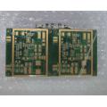
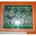
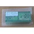
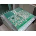
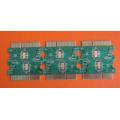
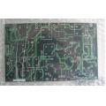
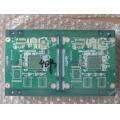
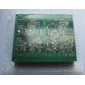
Welcome to ECBAY
Via in pad PCB
Via in pad PCB

1). 80 *190mm/2up, FR-4
2). 6 layers at 1.4mm thick
3). 35 um copper weight
4). Green solder mask LPI/White legend
5). ENIG surface finish
6). Blind via from Layer 1 to layer 2
7). Via in pad plugged conductive resin

Ads by Google

Related Searches

About Us | Contact Us | Help | Terms & Conditions
Hot Products: A | B | C | D | E | F | G | H | I | J | K | L | M | N | O | P | Q | R | S | T | U | V | W | X | Y | Z | 0-9
Copyright Notice @ 2008-2022 ECBAY Limited and/or its subsidiaries and licensors. All rights reserved.