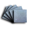
silicon wafer

We have advanced equipment and Wafer production capacity, reliable property and outstanding quality ensure high EFF solar cells.
| 125 Mono crystalline Wafer Specification |
| Growth Method | CZ |
| Conductive Type | P |
| Dopant | B |
| Orientation | 100 |
| Off Orientation | ±3° |
| Resistivity(ρ) | 0.5 3 Ω·cm or 3- 6 Ω·cm |
| Minority Carrier Lifetime | ≥10μs |
| Oxygen Content (Oi) | ≤1.0*1018 /cm3 |
| Carbon Content(C) | ≤5.0*1016 / cm3 |
| Dimension | 125*125±0.5mm |
| Diagonal | 150±0.5mm |
| Square Sides Angle | 90±0.5° |
| Streight Sections Length Deviation | 21.25±1mm |
| Thickness | 200±20 μm |
| TTV | ≤30μm |
| Saw Mark | ≤20μm |
| Warp | ≤75μm |
| Chips | Depth<0.3mm;Length<0.5mm |
| Appearance | No Stain, No Pinhole and Cracks by Visual Inspection |
silicon wafer