
1.Electronic PCBA 2.Turnkey PCBA service, SMT & DIP PCBA,PCBA Clone, 3.PCB produce with assembly 4.Design PCB gerber file
One-stop pcb assemblies service, We can offer 1 to 12 Layer PCB fabrication, PCB design, PCB layout, PCB manufacturing, PCB Assemblies, components sourcing, PCBA Function Test, design solution.
PCB Specification providing OEM service to all sorts of printed circuit board assembly | ||
1 | Layer | 1-10layer |
2 | Material | FR-4,CEM-1,CEM-3, FR-1,FR-2 |
3 | Board thickness | 0.4mm-3.5mm |
4 | Max.finished board side | 1200mm*600mm |
5 | Min.drilled hole size | 0.4mm |
6 | Min.line width | 0.1mm(4mil) |
7 | Min.line spaceing | 0.1mm(4mil) |
8 | Surface finish/treatment | HALS/HALS lead free,Chemical tin,Chemical Gold,Immersion gold Inmersion Silver/Gold,Osp,Gold Plating |
9 | Copper thickness | 0.5oz Min.,4.0oz Max |
10 | Solder mask color | green/black/white/red/blue/yellow |
11 | Inner packing | Vaccum packing,Plastic bag |
12 | Outer packing | standard carton paking |
13 | Hole tolerance | PTH:±0.075,NTPH:±0.05 |
14 | Certificate | UL,ISO9001,ISO14001,ROHS,SGS |
15 | profiling punching | Routing,V-CUT,Beveling |
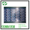
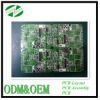
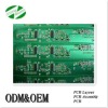
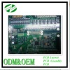
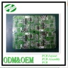
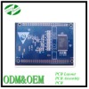
Electronic PCBA products
We supply complete PCB Assembly services including PCB & material purchasing, SMT, testing, packing, delivery.
We offer good quality warrantee, shipping lead time guarantee and lower price guarantee for all over the world.
After we get customers' product design idea(ODM)/ Gerber file & BOM list(OEM), we could offer full PCB Assembly services as below:
1 Product design and development;
2 PCB making according to PCB design;
3 Material Purchasing as BOM offered;
5 SMT/Through hole assembly;
6 Testing;
Inside circuit testing finds out every problem from manufacturing or material itself.
7 Boards cleaning;
8 Mechanism Assembly;
9 Packaging: Burble bags & seperate box /carton
10 Quick &Safe Delivery.
SMT Production Flow:
Material Receiving → IQC → Stock → Material to SMT → SMT Line Loading → Solder Paste/Glue Printing → Chip Mount → Reflow → 100% Visual Inspection → Automated Optical Inspection (AOI) → SMT QC Sampling → SMT Stock → Material to PTH → PTH Line Loading → Plated Through Hole → Wave Soldering → Touch Up → 100% Visual Inspection → PTH QC Sampling → In-Circuit Test (ICT) → Final Assembly → Functional Test (FCT) → Packing → OQC Sampling → Shipping
Lead time of prototype: 1. 10-15days, with customers completed technical information.2. 12-18days, with customers samples 3. 20-25days, with customers request and our new designProduction period: 15-20days (5 more days for trial order)
We customize various LED dimmer as per customer's requirements. If you are interested, pls feel free to contact me.
If you send us your Gerber Files and PCB specifications, we will quote for you within 12 hours
We always try our best! So we do, we conquer, and we get there!
Try us!
Electronic manufacturing service