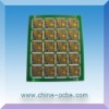
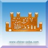
4-layer PCB with Impedance Control and 1mm Minimum Trace Size


1 Circuit electronic board PCB 2 One-stop service: design, PCB fabrication, PCB Assembly, 3 Testing, housing, turnkey, etc
Key Specifications/Special Features:
Thickness: 1.6mmMinimum trace size: 0.1mmMinimum drill: 0.15mmBlind and buried holesLayer: 4-layerBoard finished thickness: 0.2 to 7.0mmMaterial: FR-4Maximum finished board sizes: 150x 180mmMinimum hole size: 4mil (0.1mm)Minimum trace width/space: 3mil/3milCopper thickness: 0.5 to 6ozCopper thickness in hole: >18umInner packing: vacuum packing/plastic bagOutline tolerance: ±0.13mmHole size tolerance: PTH: ±0.076mmNPTH: ±0.05mmWith UL and TS16949:2002 marksSpecial requirements: impedance control,Profiling: punching, routing, V-cut and bevelingProvides OEM services to all sorts of printed circuit board assembly as well as electronic encased productsPrimary Competitive Advantages:
Electronic LinkExperienced StaffGuarantee/WarrantyPriceProduct FeaturesProduct PerformancePrompt DeliveryQuality ApprovalsReputationServiceSmall Orders AcceptedMain Export Markets:
Eastern EuropeNorth AmericaCentral/South AmericaAsiaWestern EuropeAustralasia4-layer PCB with Impedance Control and 1mm Minimum Trace Size