
1:Components scourcing from factory 2:production in china 3:PCB assembly for high complex products 4:NO MOQ limited
PCBA Features: PCB design &manufacture 1) Fabrication data inputs: Gerber data RS-274-X or RS-274-D with aperture list and drill files; Design file with Protel, PAD2000, POWERPCB, ORCAD 2) Material: FR-4, High Tg Fr4, high frequency board (Teflon, Rogers, Arlon), Halogen free, rigid-flexible board 3) Board thickness: 0.21-6.0mm 4) Layer counts: 2-16 layers 5) Surface finishes: HASL, lead-free HASL, immersion gold, gold finger, gold Plating, OSP 6) Min. Line width/spacing: 4/4mil 7) Min. Hole size: 0.25mm 8) Min. Solder mask gap between dam: 4mil 9) Max. Panel size: 20" x 30" 10) PCBA design and making basing on samples or BOM and PCB files 11) We also can reverse PCB for you according to your samples 12) Consumer, computer, communication, industrial, security, power, traffic control board SMD, DIP, AI OEM/ODM assembly. Complete product including plastics, metal works, microchip progrmming and functional testing ISO9001/9002 cerfication process Small order, high-mixed accept turn-key service including components procurement, produce, quality check, package, logistics.
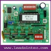
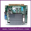
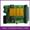
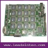
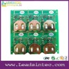
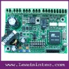
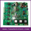
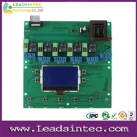
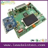
Telecom Control Board PCBA