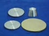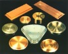

1.Purity:99.9 - 99.999% 2.Element:Copper and Copper alloy 3.Target Shape:plate,wafer,rectangular,square,circle,tube,etc. Sputtering is a PVD method for manufacturing thin films by means of evaporating solid target material (the so called sputtering target) by means of an erosive plasma and depositing the evaporated target material onto the surface of the substrate forming a thin film layer. Name: Copper sputtering target, Copper target, Copper alloy sputtering argetPurity: 99.9 - 99.999% Element: Copper and Copper alloyTarget Shape: plate, wafer, rectangular, square, circle, tube, step wafer, step rectangle, and customer tailored.
Copper Sputtering Targets,Copper target | |||
Material |
| Purities | Application |
Cu | Copper | 4N5, 5N | Electronics & Semiconductor |
Cu | Copper | 4N, 4N7 | Displays |
Cu | Copper | * | Glass Coating |
CuAl | Copper Aluminium | * | Glass Coating |
CuCr | Copper Chromium | 3N5 | Electronics & Semiconductor |
CuGa | Copper Gallium | 4N | Photovoltaics |
CuIn | Copper Indium | 4N | Photovoltaics |
CuNi | Copper Nickel | 3N5 | Electronics & Semiconductor |
CIG | Copper Indium Gallium | 4N | Photovoltaics |
other Cu | Copper / Copper alloys | * | others |
Copper Sputtering Targets