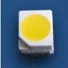
810nm Chip

1.AlGaAs/AlGaAs Wafer 2.Very high powe 3.High performance 4.Superior thermal stability
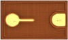
Physical Structure:
Chip dimension | Chip size | 335μm*335μm |
Thickness | 180μm | |
Emission area | 320μm | |
Bonding pad | 110μm | |
Electrode | Top: P(anode) | Gold |
Backside :N(cathode) | Gold alloy | |
Surface condition | Frosted |
Electro-Optical Characteristics: (Ta=25°C):
Parameter | Forward Voltage | Reverse Voltage | Wavelength | Spectral width at halt height | Radiant Power | Rise/ Fall Time |
Symbol | VF | VR | λP | - | P0 | tr/tf |
Condition | IF=50mA | IR=10mA | IF=50mA | IF=50mA | IF=20mA | IF=50mA |
IF=200mA | ||||||
Min. | - | 5 | - | - | 1.30 | - |
Typ. | 1.50 | - | 810 | 40 | 2.30 | 25/15 |
1.80 | ||||||
Max. | 1.75 | - | - | - | - | - |
2.25 | ||||||
Unit | V | V | nm | nm | mW | ns |
810nm Chip