
1. multi-layer PCB 2.OEM/ODM 3. Certificated by ISO, SGS, UKAS, UL 4.on time delivery 5. good after - sale service
1) Layer: 1-40
2) Board finished thickness: 0.21mm-7.0mm
3) Material: FR-4, CEM-1,CEM-3, High TG, FR4 Halogen Free,Rogers
4) Max. finished board size: 23 × 25 ( 580mm×900mm )
5) Min. drilled hole size: 3mil (0.075mm)
6) Min. Line width: 3mil (0.075mm)
Min.Line spacing:3mil (0.075mm)
7) Surface finish/treatment : HASL / HASL lead free,HAL, Chemical tin,Chemical Gold, Immersion Silver/Gold,OSP,Gold plating
8) Copper thickness: 0.5-7.0 OZ
9) Solder mask color: green/yellow/black/white/red/blue
10) Copper thickness in hole: >25.0 um (>1mil)
11)Inner packing: Vacuum packing / Plastic bag
Outer packing: Standard carton packing
12) Shape tolerance: ±0.13
Hole tolerance: PTH: ±0.076 NPTH: ±0.05
13) Certificate: UL, ISO 9001, ISO 14001,SGS , RoHS
14) Special requirements: Buried and blind vias+controlled impedance +BGA
15) Profiling: Punching, Routing, V-CUT, Beveling
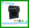
16) Provides OEM services to all sorts of printed circuit board assemblies as well as electronic encased products
Major PCB parameters below can all be customised:
1) Layers, size, thickness
2) Base material : FR4,CEM3
3) Solder mask: Red, Green,Yellow,Blue or others
4) Characters: White(default) or others
5) Surface technique: Tin soldering, plating gold, immersion gold,OSP
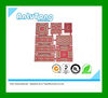
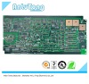
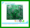
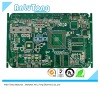
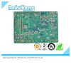
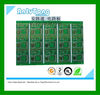
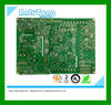
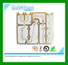
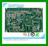
Multi-layer PCB