
Scanning Electron Microscope Electro-optical system Signal reception processing and display system Vacuum System
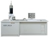
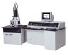
2800B Scanning Electron Microscope
Electro-optical system
Signal reception processing and display system
Computer and software systems
Vacuum System
Electro-optical systems
1.Electron gun
The type of electron gun:
(1)FEG(Field Emission Gun )
(2)W filament(Tungsten filament gun )
Tungsten filament gun works
3 pole hair fork-tungsten cathode electron gun
Self-bias, bias resistor adjustable
Added to between the gate and the anode , a continuously adjustable from 0 to 30KV negative high voltage
providing a tiny high-brightness electron source and obtaining a stable high-brightness beam.
Mechanical alignment system
2.Electromagnetic beam alignment system
3. 2 condenser lens
4.Objectives lens
Lens is used to focus images ,its Structure is a more specific .It accommodates scanning coil and elimination astigmatism component,to effectively reduce the sample's surface magnetic field ;aperture is on the top of lower pole shoes,so that beam spot size down to focus on the minimum size of the sample . The vertical distance from lower pole shoes to sample surface is called the working distance -WD
Requires a long working distance, a low spherical aberration coefficient and a small magnetic flux leakage.
5.Eliminate astigmatism
As the processing error, or a winding core in the non-uniform magnetic field asymmetry which can damage the magnetic lens symmetry ,so that it makes an oval beam spot into a spot instead of the standard round spot .It is called astigmatism .
Eliminate astigmatism correction is used to provide a weak field on the image astigmatic correction.
Eliminate astigmatism in the scanning device mounted inside the coil components.
There are X, Y pairs of images in both directions for a more positive astigmatism.
6.Scanning coils
Using X, Y two directions of magnetic deflection coil.Electron beam scans the sample was raster-like .That is, X direction of scan (line scan) and the Y direction of scan (frame scanning).
SEM was taken point by point imaging method ,Tube of the electron beam scanning and display the scanning electron beam is strictly synchronous ,therefore, the image on the display screen is a enlarging image scanned on the sample area .
Magnification of scanned images is determined by the current flowing through the coil, The larger the current, the greater the angle of scan ,then the lower image magnification. In a given scan angle, the working distance increases, the lower magnification.
7.Specimen chamber
The specimen chamber installed in the vibration-isolation frame ,Electro-optical tube installed in the top of the specimen chamber ,Vacuum system is installed below the specimen chamber.
Specimen stage from the front door into the specimen chamber, specimen chamber deflation does not affect the vacuum tube.
Chamber provides a large space, but also to annex to install convenience.
Specimen stage is so large enough range of movement that it can be used to observe a large specimen.
Specimen stage to carry out a five-dimensional movement: X, Y, Z, rotation, tilt, etc.
Specimen stage have sufficient machining accuracy to achieve micron-level mobile.
8.Signal reception processing and display system
Electronic signal from the specimen out through the grid into the detection system. When the grid added +300 V, it can effectively collect low-energy secondary electrons, when the grid added-100V voltage, collecting less than a secondary electron. However, due to higher energy backscattered electrons,are still part of the direct scintillator were collected . So when the grid with 300V, the read secondary electron image.When the grid add-100V, the probe can be observed backscattered electron image.
10KV high voltage conductive layer increases, the purpose is to improve the detection efficiency. Accelerated the secondary electrons hit scintillator to generate photoelectron,The photoelectron through the tube to the photomultiplier tube ,Photomultiplier tubes transform light signals into electrical signals ,Via pre-amplifier , a weak electrical signal will be amplified and sent to video amplifier,Then the output sent to the image on the imaging system.
Image output mode:Monitors to observe or photograph.
Magnification
When the incident electron beam to raster scan ,If the electron beam scans the specimen surface, the magnitude of As,In the cathode-ray screen simultaneously scan amplitude Ac, The SEM magnification as follows: M=Ac/As
Resolution
SEM resolution is the main performance index. In terms of micro-area composition analysis,It refers to sub Analysis of the minimum zone; Right image, it is the means to distinguish between a minimum distance between two points. Resolution size is determined by the incident electron beam diameter and the type of joint decision-modulated signal. Electron beam diameter, the smaller the higher the resolution. However, the physical signal for the imaging is different ,For example, secondary electron and backscattered electron, in the launch of the scope of the specimen surface is not the same, thus affecting its resolution. General secondary electron image resolution is about 5-10nm, backscattered electron image resolution of about 50-200nm.
9. Computer and software systems
1.It is a part of the electrical control.
2.Automation and intelligence is an important characteristic of modern instruments.
3.Make the operation of electronic microscope convenient.
4.To achieve office network and automation.
10. Vacuum system
1.Provide vacuum which electro-optical system requirements
2.Vacuum systems include:Mechanical vacuum pumps and high vacuum pumps, vacuum 3.alves, vacuum vibration-isolation, vacuum measurement, Etc.
4.Automatic protection function.
SPECIFICATION
Resolution 4.5nm (Tungsten filament)
Magnification 15×~250,000×
Electron Optical System 1.Electron gun:Tungsten cathode 2.Accelerating voltage :0---30kV 3.Lens system :Three electron magnetic lens system 4.Objective lens aperture:Three apertures selectableScanning Electron Microscope