
main joint material for semiconductor packaging
Copper bonding wire is a kind of material for inner lead with excellent electrical, thermal, mechanical properties and excellent chemical stability, mainly for ket materials of semiconductor packaging( molding compound, solder ball, high-density packaging substrate, conducting resin).
Product Advantage
1. Material costs:low
2. Conductivity: much thinner bonding wires during fine pitch packaging, excellent performance of fine pitch
(much smaller bonding pad), improving current capacity and property of power regulating
device.
3. Thermal conductivity: 39.5KW/m2K
4. Mechanical properties: high mechanical property, larger tensile strength, better elongation, excellent ball
collar strength and higher arc stability.
5. Stability: stable-slow inter-metallic growth rate, improving mechanical stability and decreasing incremental
resistance: moderate IMCgrowth enables bonding strength to be improved.
6. Solder joint: significantly reduced inter-metallic growth rate of solder joints. Resistance reduced, heat
production decreased, bonding reliability devece performance improved. As the new products
have their inter- metallic growth rate, resistance and heat production lower than gold wire,
the amount of resistance increase with time and aging rate also is reduced.
Diameter(mm)
| 0.018 | 0.020 | 0.023 | 0.025 | 0.028 | 0.030 | 0.032 | 0.033 | 0.038 | 0.050 |
special order avaliable
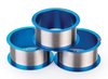
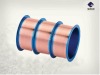
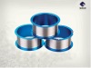
copper bonding wire