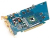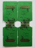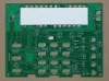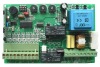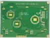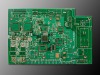

pcb layout design 1.pcb assembly ,components procure,pcb test 2.Competetive price with good quality 3.OEM&ODM service PCB layout designComplete electronic product design from concept to completion: This involves the development of a full fledged, complete "ready to market" product and consists of enclosure design (either based on readily available enclosures, or custom designed mold preparation), hardware design (schematic & PCB design), user interface design (front panel/control panels), firmware/software design, product approvals (CE mark, FCC, UL etc). We are good at converting mere English descriptions into complete products by interacting with clients till we understand what they have in mind. PCB (printed circuit board) design & prototyping (single & multilayer): The printed circuit board, "PCB", is an inherent part of every electronic hardware. Every custom electronics hardware that we design includes PCB layout designing, prototyping & assembly by default. We can also offer PCB layout designing (PCB designing for short) & prototyping as a standalone service in order to convert any existing schematic diagrams that you might have already designed into fully assembled prototypes.
A.
1 Layer: 1-30
2 Board finished thickness:0.21mm-7.0mm
3 Material: FR-4,CEM-1,CEM-3,High TG,FR4 halogen Free,Rogers
4 Max.finished board size:580*900mm
5 Min.drilled hole size:3mil(0.075mm)
6 Min.Line width:3mil(0.075mm)
Min.Line spacing:3mil(0.075mm)
7 Surface finish/treatment: HASL/HASL lead free,HAL,Chemical tin,Chemical Gold,Immersion Silver/Gold,OSP, Gold plating.
8 Copper thickness:0.5-3.0oz
9 Solder mask color: Green/yellow/black/white/red/blue
10 Copper thickness in hole: >25.0 um(>1mil)
11 Inner packing: Vaccum packing/Plastic bag
Outer packing: Standard carton packing
12 Shape tolerance:±0.13
Hole tolerance:PTH: ±0.076 NPTH: ±0.05
13 Cerificate: UL.ISO9001.ISO14001.SGS.ROHS.
14 Special requirements:Buried and blind vias+Controlled impedance+BGA
15 Profilling:Punching.Routing.V-CUT.Beveling
16 Provides OEM Services to all sorts of printed circuit board assembly as we as electronic encased products.
B.Needed
1.Gerber file and BOM
2.Clear photos of pcba or pcba sample deliver to us
3.Your test method
pcb layout design service